Valence Band Offset
Scalar Electronic
The valence band offset (VBO) is the energy difference of the valence band edges \(\varepsilon_{v}\) across a heterostructure interface.
Note, that the VBO is not simply given by the difference of valence band maxima of the two materials, but also depends
on the electronic distribution at the interface.
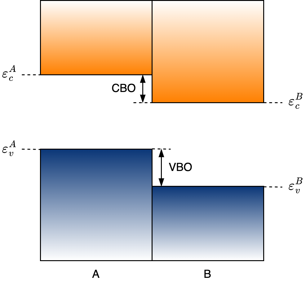 Regarding conduction band edges \(\varepsilon_{c}\) there exists an equivalent property, termed conduction band offset (CBO).
The VBO plays an important role for the transport properties of charge carriers in heterojunction devices (e.g. hole injection efficiency). Using first principles calculations, the VBO can be determined through the potential lineup method 123 or via the local density of states (LDOS) 3. For more details regarding the potential lineup method, see also the valence band offset tutorial
Example
Its value can be estimated using the valence band offset workflow, and it is returned under the Results Tab interface with the following appearance (in eV).
0.250
Schema
The JSON schema and an example representation for this property can be found here.
Links
-
A. Baldereschi, S. Baroni, R. Resta, Phys. Rev. Lett. 61, 734 (1988); DOI: 10.1103/PhysRevLett.61.734 ↩
-
L. Colombo, R. Resta, S. Baroni, Phys. Rev. B 44, 5572 (1991); DOI: 10.1103/physrevb.44.5572 ↩
-
M. Peressi, N. Binggeli, A. Baldereschi, J. Phys. D: Appl. Phys. 31, 1273-1299 (1998); DOI: 10.1088/0022-3727/31/11/002 ↩↩