Calculate Valence Band Offset
This tutorial page explains how to calculate the valence band offset (VBO) based on the potential lineup method123 using Density Functional Theory. For this tutorial, we consider a 2D material interface MoS2/WS2 and use Quantum Espresso as our main simulation engine. The content of this tutorial was also part of our 2021 webinar 2D Materials and their Electronic Properties4
Simulation engines considered in this tutorial
The workflow presented in this tutorial is currently only available for Quantum ESPRESSO.
Definitions
Valence Band Offset
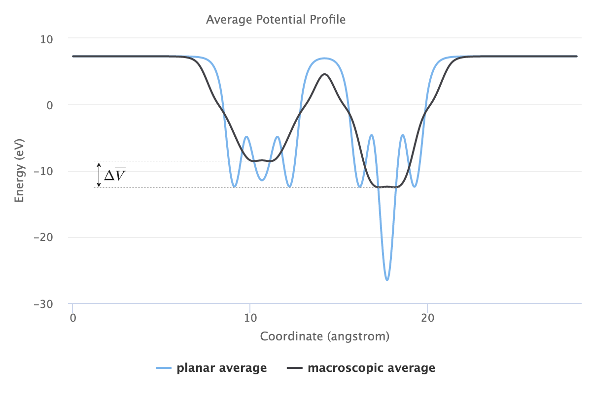
The valence band offset is defined by the relative position of the valence band on both sides of the interface. This property is relevant to study the charge transport across interfaces such as semiconductor heterojunctions. Other properties related to the band profile at the interface are the conduction band offset and Schottky barrier (metal-semiconductor interface).
Potential Lineup Method
This tutorial employs the potential lineup method in order to determine the valence band offset, which requires the calculation of the macroscopically averaged electrostatic potential and valence band maximum of the two materials. The valence band offset for an A/B interface can then be determined via:
The first term, \(\Delta E_{v}\), is usually referred to as the band structure term and defined as the difference of the two valence band maxima \(\varepsilon_{v}\) referenced to the macroscopically averaged electrostatic potential \(\overline{V}\) in each material:
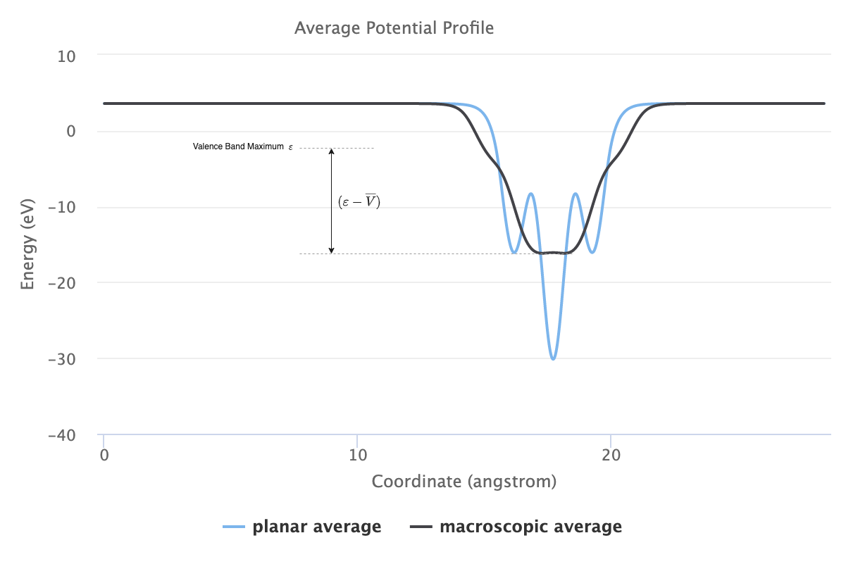 The second term, \(\Delta \overline{V}\), is determined from the lineup of the macroscopically averaged electrostatic potential in
the interface heterostructure.
The second term, \(\Delta \overline{V}\), is determined from the lineup of the macroscopically averaged electrostatic potential in
the interface heterostructure.
Choose Materials
When creating the job, the user needs to select three materials corresponding to the MoS2/WS2 interface and the isolated monolayers of both MoS2 and WS2. Each of the structures is expected to be relaxed. The initial interface structure was taken from materialsproject and optimized via a variable-cell relaxation of the x- and y-components. The monolayer structures were extracted from the interface and optimized in the same way. The final structures are available on the Mat3ra platform:
Order of Materials
The VBO workflow assumes the interface structure to correspond to the first material, i.e. please be sure to load the interface structure first.
Choose Workflow
The workflow for calculating the valence band offset can be imported from the Workflows Bank into the account-owned collection. This workflow can later be selected and added to the Job being created. A representation of this workflow is also available as part of the Mat3ra workflow definitions repository (wode.js).
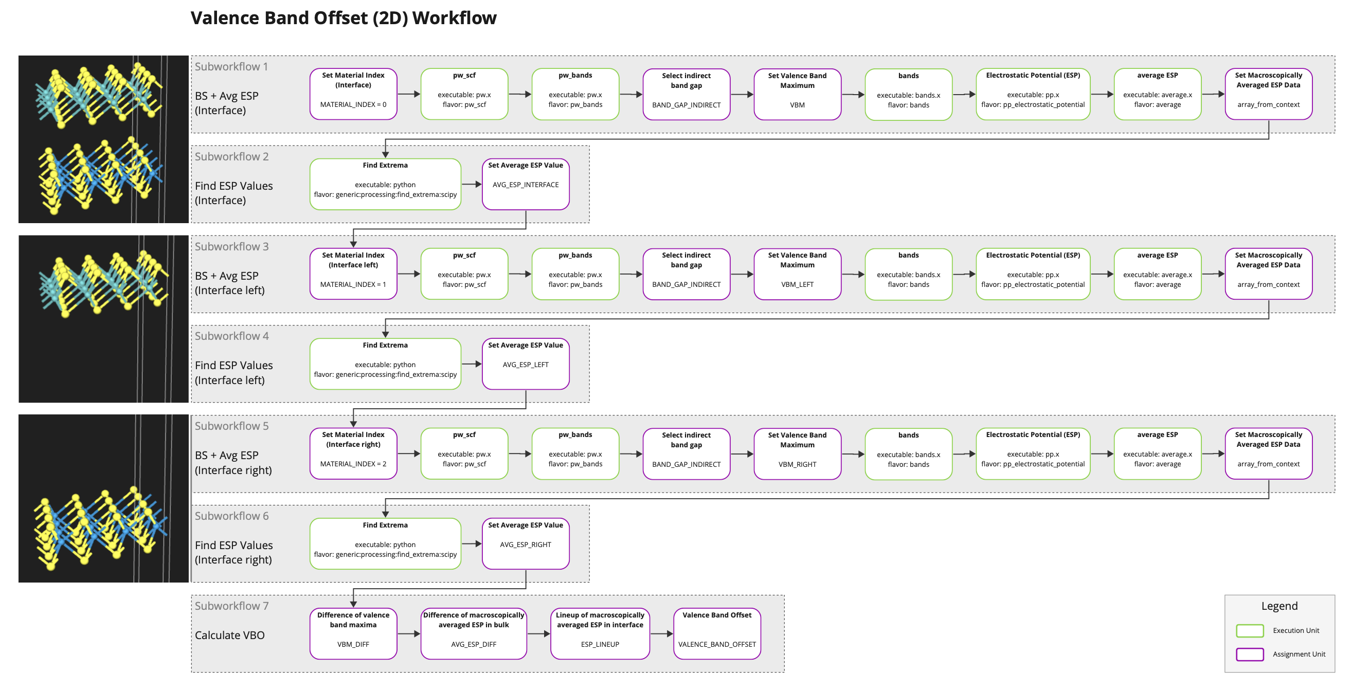
The workflow contains two subworkflows per material calculating the valence band maximum (via band structure), macroscopically averaged electrostatic potential, and its minima. As the system in this tutorial is a heterostructure built of monolayers, determining the value of the macroscopically averaged electrostatic potential in the region of the monolayer corresponds to finding the minima of \(\overline{V}\). For multilayered heterostructures the problem becomes equivalent of finding plateaus of \(\overline{V}\). The final subworkflow collects all the intermediate results and determines the value of the valence band offset.
Workflow Settings
For the purpose of this tutorial, we set the size of the grid of k-points to 6 x 6 x 1 for each of the three PW-SCF units and adjust the k-path to reflect the reduced dimensionality (Γ-M-K-Γ). In addition, one should also adjust the size of the window for macroscopic averaging. For the present system we set this size to the distance between the sulfur atoms in both monolayers (ca. 5.7 bohr).
Submit Job
Before submitting the job, the user should click on the "Compute" tab of Job Designer and inspect the compute parameters included therein.
Examine results
When all unit computations are complete at the end of Job execution, switching to the Results tab of Job Viewer will show the results of the simulation, including the valence band offset as well as the plots of the planar and macroscopic average of the electrostatic potentials.
Comparison with Experimental Value
The calculated value of ~0.27 eV for the valence band offset is below the experimental5 value of 0.55 eV, but agrees with previous theoretical results6 of 0.32 eV and 0.22 eV, respectively.
Animation
We demonstrate the above-mentioned steps involved in the creation and execution of a Valence Band Offset workflow in the following animation.
Links
-
A. Baldereschi, S. Baroni, R. Resta, Phys. Rev. Lett. 61, 734 (1988); DOI: 10.1103/PhysRevLett.61.734 ↩
-
L. Colombo, R. Resta, S. Baroni, Phys. Rev. B 44, 5572 (1991); DOI: 10.1103/physrevb.44.5572 ↩
-
M. Peressi, N. Binggeli, A. Baldereschi, J. Phys. D: Appl. Phys. 31, 1273-1299 (1998); DOI: 10.1088/0022-3727/31/11/002 ↩
-
2D Materials and their Electronic Properties (Mat3ra YouTube) ↩
-
C. Lu, et. al, Phys. Status Solidi A, 1900544 (2009); DOI: 10.1002/pssa.201900544 ↩
-
E. Torun, H.P.C. Miranda, A. Molina-Sánchez, L. Wirtz, Phys. Rev. B 97, 245427 (2018); DOI: 10.1103/PhysRevB.97.245427 ↩