Graphene/Ni(111) Interface Optimization.
Introduction.
This tutorial demonstrates how to create and optimize a Graphene/Ni(111) interface structure following the experimental observations presented in the literature. We will focus on finding the most energetically favorable position of graphene on the Ni(111) surface.
Manuscript
Arjun Dahal, Matthias Batzill "Graphene–nickel interfaces: a review" Nanoscale, 6(5), 2548. (2014) DOI: 10.1039/c3nr05279f. 123
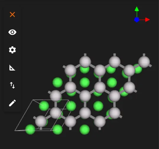
We will recreate the interface structure and optimize the film position to match the experimental findings shown in the figure below:

1. Create Interface Structure.
1.1. Load Base Materials.
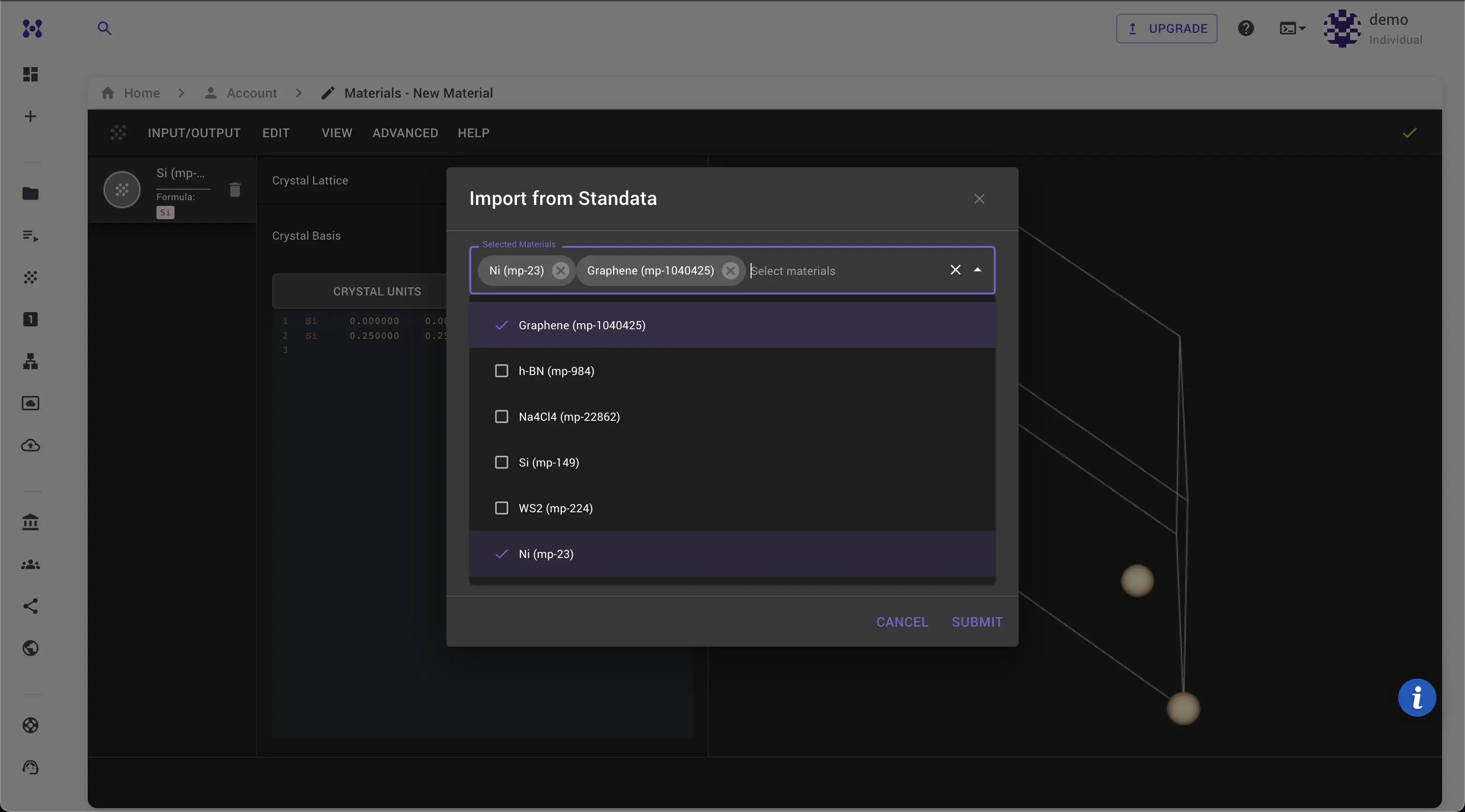
Navigate to Materials Designer and import both graphene and nickel materials from the Standata.
1.2. Launch JupyterLite Session.
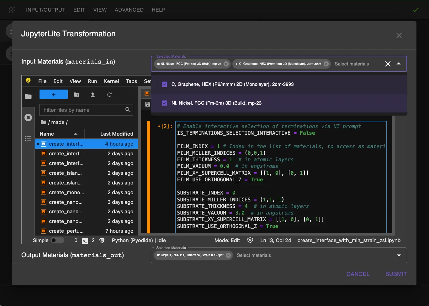
Select the "Advanced > JupyterLite Transformation" menu item to launch the JupyterLite environment.
1.3. Open create_interface_with_min_strain_zsl.ipynb notebook.
Find and open the create_interface_with_min_strain_zsl.ipynb notebook. This notebook will help us create the initial interface structure.
1.4. Set up interface parameters.
Edit the notebook parameters to create the Gr/Ni(111) interface:
# Material selection
SUBSTRATE_NAME = "Nickel"
FILM_NAME = "Graphene"

# Slab parameters
SUBSTRATE_MILLER_INDICES = (1, 1, 1)
SUBSTRATE_THICKNESS = 4  # in atomic layers
FILM_THICKNESS = 1  # in atomic layers

# Interface parameters
MAX_AREA = 50  # in Angstrom^2
INTERFACE_DISTANCE = 2.58  # in Angstrom from literature
INTERFACE_VACUUM = 20.0  # in Angstrom
1.5. Run interface creation.
Run the notebook using "Run > Run All Cells". This will:
- Create slabs from both materials
- Find the optimal lattice matching using the ZSL algorithm
- Generate the initial interface structure
2. Optimize Film Position.
2.1. Open optimize_film_position.ipynb notebook.
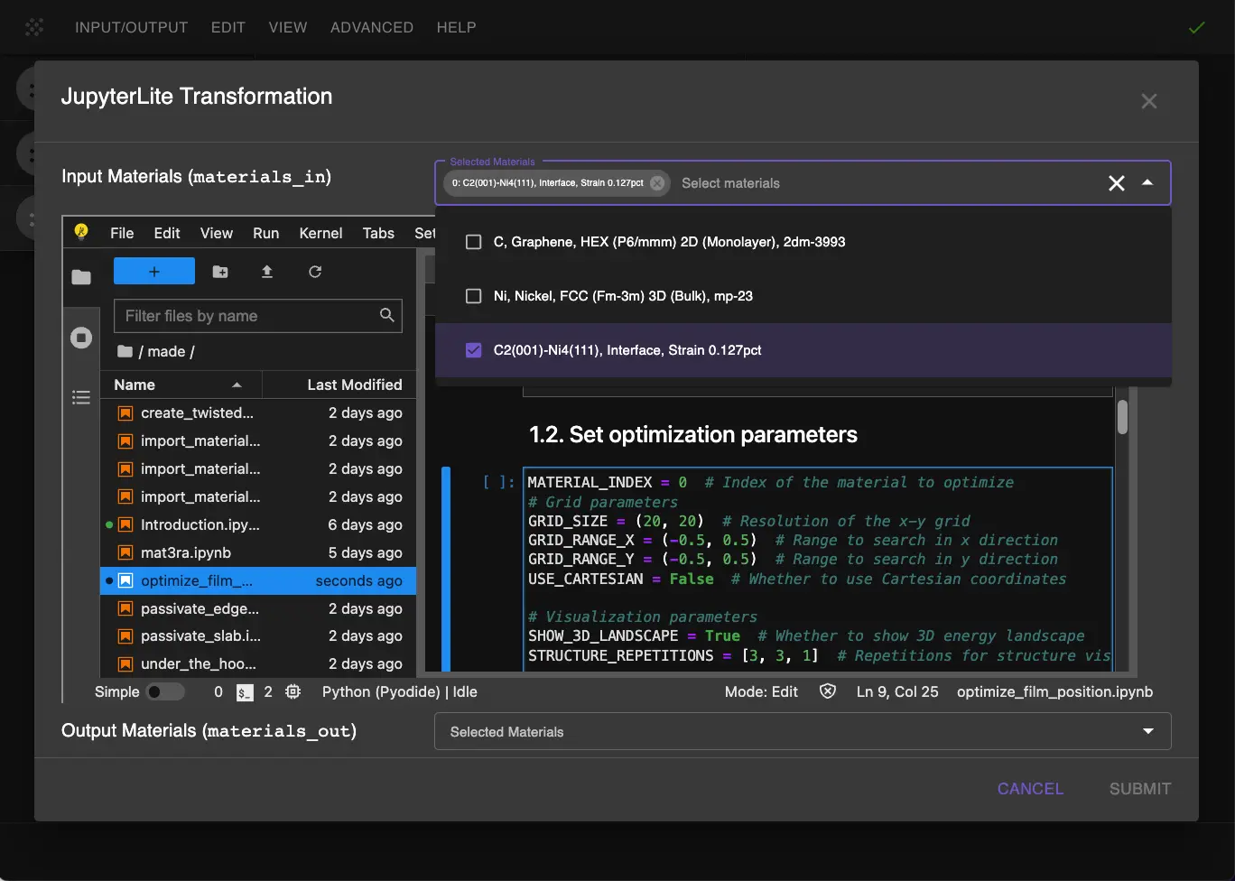
Find and open the optimize_film_position.ipynb notebook which will help us find the optimal position of the graphene layer.
2.2. Set optimization parameters.
Configure the optimization parameters:
# Grid parameters
GRID_SIZE = (20, 20)  # Resolution of the x-y grid
GRID_RANGE_X = (-0.5, 0.5)  # Range in crystal coordinates
GRID_RANGE_Y = (-0.5, 0.5)
USE_CARTESIAN = False  # Use crystal coordinates

# Visualization parameters
STRUCTURE_REPETITIONS = [3, 3, 1]
Key parameters explained:
- GRID_SIZE: Controls the resolution of position sampling
- GRID_RANGE: Search range in crystal coordinates
- USE_CARTESIAN: Set to False for hexagonal systems
2.3. Run optimization.
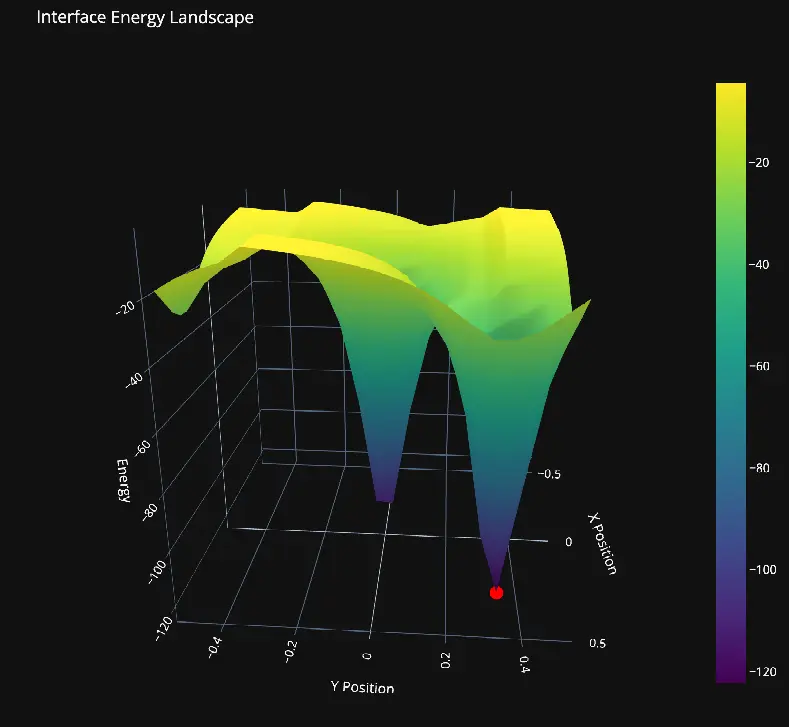
Run all cells in the notebook. The optimization will:
- Calculate energy landscape across different positions
- Find the global minimum energy position
- Generate visualizations of the results
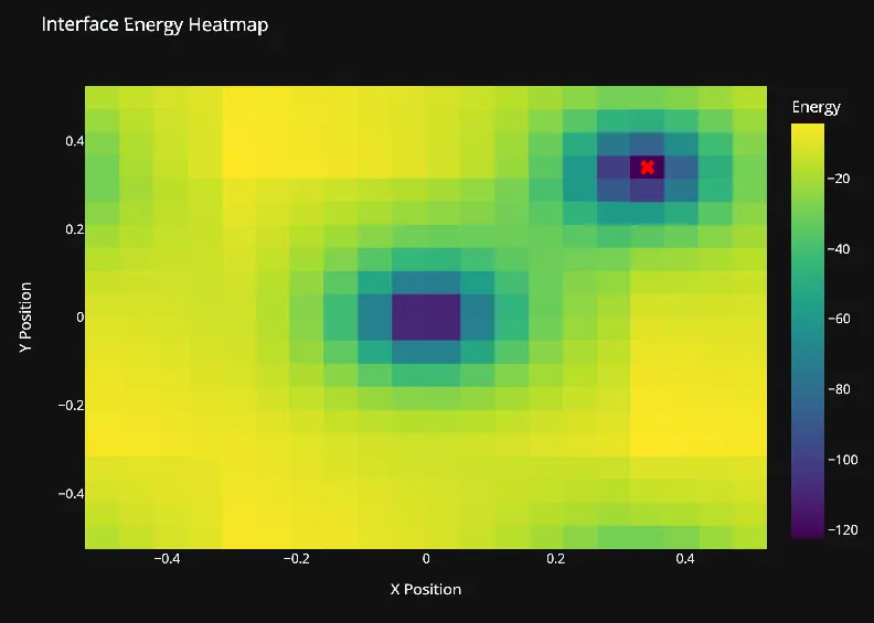
3. Analyze Results.
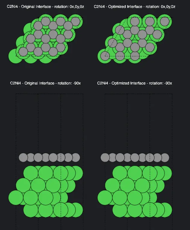
Compare the original and optimized interface structures to see the difference in the graphene position.
4. Save Optimized Structure.
The optimized interface structure will be automatically passed back to Materials Designer where you can: 1. Save it in the workspace 2. Export it in various formats (JSON, POSCAR, etc.) 3. Use it for further calculations
Interactive JupyterLite Notebook.
The following JupyterLite notebook demonstrates the complete process. Select "Run" > "Run All Cells".
Parameter Fine-tuning.
To adjust the interface optimization:
- Interface Creation:
- Adjust
SUBSTRATE_THICKNESSfor more Ni layers - Modify
MAX_AREAto control supercell size -
Change
INTERFACE_DISTANCEif needed -
Position Optimization:
- Increase
GRID_SIZEfor finer sampling - Adjust
GRID_RANGEto search different areas - Enable 3D visualization with
SHOW_3D_LANDSCAPE = True
References.
-
Arjun Dahal and Matthias Batzill. Graphene–nickel interfaces: a review. Nanoscale, 6:2548–2562, 2014. URL: https://doi.org/10.1039/C3NR05279F. ↩
-
Y. Gamo, A. Nagashima, M. Wakabayashi, M. Terai, and C. Oshima. Atomic structure of monolayer graphite formed on ni(111). Surface Science, 374(1-3):61–64, 1997. URL: https://www.sciencedirect.com/science/article/abs/pii/S0039602896007856. ↩
-
G. Bertoni, L. Calmels, A. Altibelli, and V. Serin. First-principles calculation of the electronic structure and eels spectra at the graphene/ni(111) interface. Physical Review B, 2004. URL: https://journals.aps.org/prb/abstract/10.1103/PhysRevB.71.075402. ↩